Photolithography is a crucial technology in semiconductor fabrication used to transfer intricate circuit patterns onto silicon wafers. This process involves coating the wafer with a light-sensitive photoresist, exposing it to ultraviolet light through a photomask, and developing the exposed areas to create a patterned surface. The resulting pattern guides the etching and doping steps that form transistors and other semiconductor devices essential for integrated circuits. In modern semiconductor manufacturing, extreme ultraviolet (EUV) photolithography enables the creation of features smaller than 10 nanometers, improving chip density and performance. Companies like Intel and TSMC extensively utilize photolithography to achieve Moore's Law scaling, producing high-performance CPUs and GPUs. Photolithography data, such as resolution limits and overlay accuracy, directly influence yield and device reliability throughout the semiconductor production cycle.
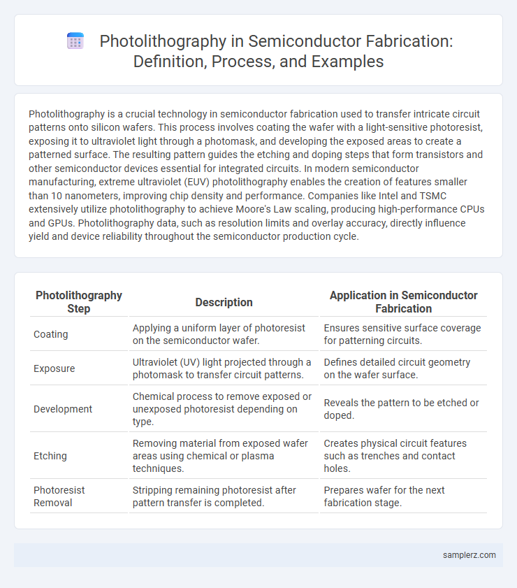
Table of Comparison
| Photolithography Step | Description | Application in Semiconductor Fabrication |
|---|---|---|
| Coating | Applying a uniform layer of photoresist on the semiconductor wafer. | Ensures sensitive surface coverage for patterning circuits. |
| Exposure | Ultraviolet (UV) light projected through a photomask to transfer circuit patterns. | Defines detailed circuit geometry on the wafer surface. |
| Development | Chemical process to remove exposed or unexposed photoresist depending on type. | Reveals the pattern to be etched or doped. |
| Etching | Removing material from exposed wafer areas using chemical or plasma techniques. | Creates physical circuit features such as trenches and contact holes. |
| Photoresist Removal | Stripping remaining photoresist after pattern transfer is completed. | Prepares wafer for the next fabrication stage. |
Introduction to Photolithography in Semiconductor Fabrication
Photolithography is a crucial process in semiconductor fabrication that uses light to transfer geometric patterns from a photomask onto a silicon wafer coated with photoresist. This technique enables the creation of intricate circuit designs with nanoscale precision, essential for manufacturing integrated circuits and microchips. Key parameters include wavelength of light, photoresist sensitivity, and exposure time, all of which determine the resolution and accuracy of the resulting semiconductor devices.
Key Steps in the Photolithography Process
The photolithography process in semiconductor fabrication involves coating the silicon wafer with a photoresist layer that is sensitive to ultraviolet (UV) light. Precise UV light exposure through a photomask transfers the circuit pattern onto the photoresist, followed by a development step that removes either the exposed or unexposed photoresist depending on its type. Subsequent etching and photoresist stripping reveal the patterned wafer surface, enabling the creation of intricate semiconductor device structures.
Positive vs. Negative Photoresist Applications
Positive photoresist in photolithography becomes soluble when exposed to ultraviolet light, allowing precise pattern transfer for creating intricate semiconductor circuits such as transistor gates. Negative photoresist hardens upon exposure, making it suitable for fabricating microelectromechanical systems (MEMS) and robust mask layers in integrated circuit manufacturing. These distinct properties optimize pattern fidelity and process efficiency in advanced semiconductor fabrication workflows.
Spin Coating Techniques for Photoresist Application
Spin coating techniques in photolithography are crucial for uniformly applying photoresist layers on semiconductor wafers, enabling precise pattern transfer during microfabrication. The process involves depositing a liquid photoresist onto a wafer and spinning it at high speeds to create a thin, even film essential for defining intricate circuit features. Optimizing spin speed, acceleration, and time directly affects film thickness and uniformity, which are critical parameters in advanced semiconductor device manufacturing.
UV Exposure and Mask Alignment in Pattern Transfer
UV exposure in photolithography plays a crucial role in semiconductor fabrication by selectively hardening the photoresist layer through controlled ultraviolet light projection. Precise mask alignment ensures that the circuit patterns from the photomask accurately overlay the wafer surface, enabling high-resolution pattern transfer critical for creating integrated circuits. This combination of UV exposure and mask alignment achieves sub-micron feature definition essential for modern semiconductor devices.
Development Process: Revealing the Circuit Patterns
Photolithography in semiconductor fabrication involves coating the silicon wafer with a light-sensitive photoresist, which is then exposed to ultraviolet light through a photomask containing the intricate circuit patterns. The exposed areas of the photoresist undergo a chemical reaction, allowing selective development that reveals the underlying substrate in precise patterns. This process enables the transfer of microscopic geometries necessary for creating integrated circuits with nanoscale features in modern microchips.
Examples of Photolithography in Integrated Circuit Manufacturing
Photolithography is essential in integrated circuit manufacturing for defining intricate circuit patterns on silicon wafers with high precision. Techniques such as deep ultraviolet (DUV) lithography enable the creation of feature sizes below 50 nanometers, critical for advanced microprocessors and memory chips. Immersion lithography further enhances resolution by using a liquid medium between the lens and wafer, supporting the production of cutting-edge semiconductor devices.
Deep UV Lithography in Advanced Semiconductor Nodes
Deep UV lithography employs wavelengths around 193 nm to achieve critical feature sizes below 50 nm in advanced semiconductor nodes, enabling high-resolution patterning essential for modern microprocessors. This technique uses excimer lasers and specialized photoresists to precisely transfer intricate circuit designs onto silicon wafers with exceptional fidelity. Deep UV lithography remains a cornerstone in semiconductor fabrication, balancing resolution, throughput, and cost before extreme ultraviolet (EUV) lithography becomes widespread.
Common Defects and Quality Control in Photolithography
Photolithography in semiconductor fabrication often encounters common defects such as pattern misalignment, CD (critical dimension) variation, and photoresist residues, which can severely impact transistor performance and yield. Advanced quality control techniques include in-line defect inspection systems using electron microscopy and scatterometry to detect and quantify defects at nanoscale resolution. Data-driven process control leveraging machine learning algorithms further enhances yield by predicting defect formation and optimizing exposure parameters in real time.
Future Trends: EUV Lithography and Semiconductor Scaling
Extreme Ultraviolet (EUV) lithography represents the forefront of semiconductor fabrication, enabling feature sizes below 7 nanometers by utilizing shorter wavelengths around 13.5 nm for higher resolution patterning. Future trends focus on improving EUV source power and mask defect control to sustain Moore's Law through advanced semiconductor scaling. Innovations in multiple patterning techniques combined with EUV lithography drive the production of increasingly dense, high-performance integrated circuits critical for next-generation electronic devices.
example of photolithography in semiconductor fabrication Infographic