A monolayer in semiconductor technology refers to a single, atomically thin layer of material used in device fabrication. Graphene, a monolayer of carbon atoms arranged in a hexagonal lattice, exemplifies this concept due to its exceptional electrical conductivity and mechanical strength. Transition metal dichalcogenides (TMDs) such as molybdenum disulfide (MoS2) also serve as monolayers, providing semiconducting properties vital for nanoscale transistors. These monolayers enable innovations in semiconductor devices by allowing precise control over electronic and optical properties at the atomic scale. MoS2 monolayers exhibit a direct bandgap essential for efficient light emission and detection, distinguishing them from bulk counterparts with indirect bandgaps. The integration of monolayer materials into semiconductor technology supports advancements in flexible electronics, high-performance transistors, and quantum computing applications.
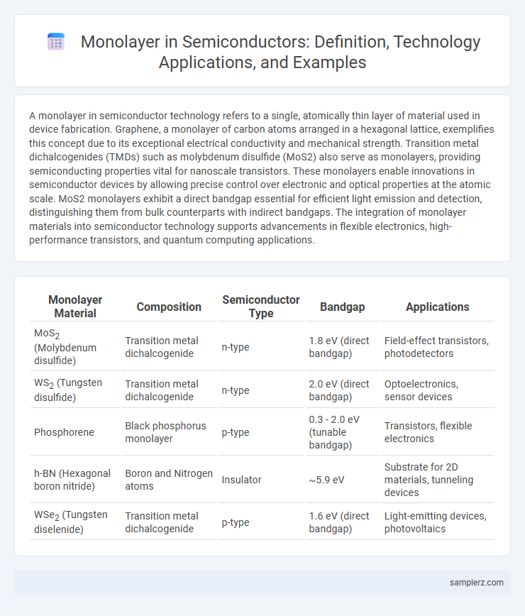
Table of Comparison
| Monolayer Material | Composition | Semiconductor Type | Bandgap | Applications |
|---|---|---|---|---|
| MoS2 (Molybdenum disulfide) | Transition metal dichalcogenide | n-type | 1.8 eV (direct bandgap) | Field-effect transistors, photodetectors |
| WS2 (Tungsten disulfide) | Transition metal dichalcogenide | n-type | 2.0 eV (direct bandgap) | Optoelectronics, sensor devices |
| Phosphorene | Black phosphorus monolayer | p-type | 0.3 - 2.0 eV (tunable bandgap) | Transistors, flexible electronics |
| h-BN (Hexagonal boron nitride) | Boron and Nitrogen atoms | Insulator | ~5.9 eV | Substrate for 2D materials, tunneling devices |
| WSe2 (Tungsten diselenide) | Transition metal dichalcogenide | p-type | 1.6 eV (direct bandgap) | Light-emitting devices, photovoltaics |
Introduction to Monolayers in Semiconductors
Monolayers in semiconductors, such as graphene and transition metal dichalcogenides (TMDCs) like MoS2, exhibit unique electronic properties due to their atomic thickness and two-dimensional structure. These monolayer materials enable enhanced electron mobility, tunable bandgaps, and strong spin-orbit coupling, which are critical for next-generation electronic and optoelectronic devices. Understanding the fundamental properties of semiconductor monolayers is essential for developing innovative applications in flexible electronics, sensors, and quantum computing.
Significance of Monolayers in Modern Electronics
Monolayers in semiconductors, such as graphene or transition metal dichalcogenides (TMDCs), exhibit exceptional electrical and optical properties crucial for developing next-generation electronic devices. Their atomic-scale thickness enables precise control over electron mobility, enabling ultra-fast transistors and highly sensitive photodetectors. The integration of monolayer materials significantly enhances device performance, energy efficiency, and scalability in modern electronics manufacturing.
Graphene: The Pioneer Monolayer Material
Graphene, the pioneer monolayer material in semiconductor technology, consists of a single layer of carbon atoms arranged in a hexagonal lattice, exhibiting exceptional electrical conductivity and mechanical strength. Its unique two-dimensional structure allows for ultra-high electron mobility, making it ideal for next-generation transistors and flexible electronic devices. Research continues to explore graphene's potential in improving semiconductor performance, energy efficiency, and device miniaturization.
Molybdenum Disulfide (MoS₂) as a Semiconductor Monolayer Example
Molybdenum Disulfide (MoS2) is a prominent example of a semiconductor monolayer, consisting of a single layer of molybdenum atoms sandwiched between two layers of sulfur atoms. This two-dimensional material exhibits a direct bandgap of approximately 1.8 eV, enabling efficient electronic and optoelectronic applications such as transistors and photodetectors. MoS2 monolayers demonstrate high carrier mobility, mechanical flexibility, and strong light-matter interaction, making them a key candidate for next-generation semiconductor technologies.
Transition Metal Dichalcogenides (TMDs) in Monolayer Form
Transition Metal Dichalcogenides (TMDs) in monolayer form, such as MoS2 and WS2, exhibit unique electronic properties including a direct bandgap that contrasts with their bulk counterparts. These monolayers enable ultra-thin semiconductor devices with excellent flexibility and high carrier mobility, making them ideal for next-generation transistors and optoelectronic applications. The strong spin-orbit coupling and valley polarization effects in monolayer TMDs further enhance their potential for innovative quantum and spintronic technologies.
Semiconductor Properties of Phosphorene Monolayers
Phosphorene monolayers exhibit exceptional semiconductor properties characterized by a direct bandgap that varies with the number of layers, typically ranging from 0.3 eV in bulk black phosphorus to approximately 2.0 eV in monolayer form. These monolayers demonstrate high carrier mobility exceeding 1000 cm2/V*s, which is significantly higher than many other two-dimensional materials like MoS2. The anisotropic electrical conductivity and strong in-plane anisotropy of phosphorene enhance its performance in field-effect transistors, making it a promising candidate for next-generation nanoelectronic devices.
Gallium Selenide (GaSe) Monolayer Applications
Gallium Selenide (GaSe) monolayers exhibit exceptional optoelectronic properties, making them ideal for applications in photodetectors, light-emitting devices, and flexible electronics. Their direct bandgap and strong light-matter interactions enable high-performance sensors and energy-efficient light sources. Integration of GaSe monolayers in semiconductor devices advances the development of ultrathin, flexible, and transparent technologies.
Hexagonal Boron Nitride (h-BN): Monolayer Insulator in Semiconductors
Hexagonal Boron Nitride (h-BN) serves as a prominent monolayer insulator in semiconductor devices due to its wide bandgap of approximately 5.9 eV, which ensures excellent electrical insulation while maintaining atomic-level thinness. Its hexagonal lattice structure closely matches that of graphene, enabling seamless integration in heterostructures for advanced nanoelectronics and optoelectronic applications. The exceptional thermal stability and chemical inertness of monolayer h-BN enhance device performance by providing effective dielectric layering and reducing charge traps in 2D semiconductor architectures.
Monolayer Heterostructures for Enhanced Semiconductor Performance
Monolayer heterostructures, such as those formed by stacking monolayers of transition metal dichalcogenides (TMDs) like MoS2 and WS2, exhibit unique electronic and optical properties critical for advanced semiconductor devices. These atomically thin layers enable precise control of band alignment and exciton dynamics, leading to improved charge carrier mobility and reduced energy consumption in transistors and photodetectors. The integration of monolayer heterostructures into semiconductor technology drives innovation in nanoelectronics and optoelectronics, enhancing device performance and efficiency.
Future Trends and Applications of Monolayers in Semiconductor Devices
Monolayers such as transition metal dichalcogenides (TMDs) like MoS2 and WS2 are revolutionizing semiconductor devices by enabling ultra-thin, flexible, and high-performance transistors with enhanced electron mobility. Future trends in semiconductor technology include the integration of these monolayer materials into nanoscale photodetectors, flexible electronics, and quantum computing components, leveraging their unique two-dimensional electronic properties. Advanced applications also focus on energy-efficient spintronic devices and next-generation sensors, exploiting the tunable bandgaps and strong spin-orbit coupling inherent in monolayer semiconductors.
example of monolayer in semiconductor Infographic