Plasmonics plays a crucial role in advancing photonic technologies by enabling the manipulation of light at the nanoscale. Key entities involved include metallic nanoparticles such as gold and silver, which support surface plasmons--coherent oscillations of electrons that enhance electromagnetic fields. Data from recent studies show that plasmonic devices can improve the efficiency of photonic circuits by concentrating light beyond the diffraction limit. In photonic applications, plasmonic structures are used to create nanoscale waveguides, sensors, and switches. Researchers utilize materials like graphene combined with metallic nanostructures to optimize plasmonic resonance for specific wavelengths. Experimental results demonstrate that plasmonic photonic components significantly reduce device size while maintaining high-speed optical signal processing capabilities.
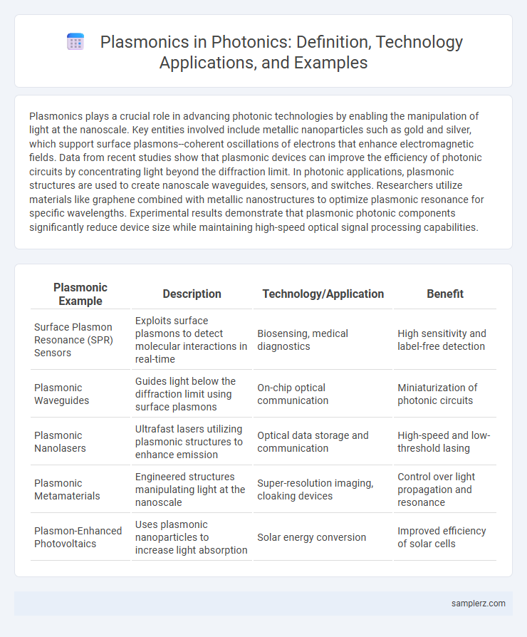
Table of Comparison
| Plasmonic Example | Description | Technology/Application | Benefit |
|---|---|---|---|
| Surface Plasmon Resonance (SPR) Sensors | Exploits surface plasmons to detect molecular interactions in real-time | Biosensing, medical diagnostics | High sensitivity and label-free detection |
| Plasmonic Waveguides | Guides light below the diffraction limit using surface plasmons | On-chip optical communication | Miniaturization of photonic circuits |
| Plasmonic Nanolasers | Ultrafast lasers utilizing plasmonic structures to enhance emission | Optical data storage and communication | High-speed and low-threshold lasing |
| Plasmonic Metamaterials | Engineered structures manipulating light at the nanoscale | Super-resolution imaging, cloaking devices | Control over light propagation and resonance |
| Plasmon-Enhanced Photovoltaics | Uses plasmonic nanoparticles to increase light absorption | Solar energy conversion | Improved efficiency of solar cells |
Introduction to Plasmonics in Photonics
Plasmonics in photonics exploits surface plasmon polaritons to confine light at the nanoscale beyond the diffraction limit, enabling enhanced optical sensing and signal processing. Metallic nanostructures, such as gold and silver nanoparticles, serve as the primary platforms for manipulating electromagnetic waves through localized surface plasmons. This integration of plasmonics with photonic devices paves the way for breakthroughs in ultra-compact optical circuits and highly sensitive biosensors.
Fundamentals of Plasmonic Phenomena
Plasmonic phenomena are based on the resonant oscillation of conduction electrons at the interface between a metal and a dielectric material, enabling confinement of light beyond the diffraction limit. Surface plasmon polaritons (SPPs) propagate along metal-dielectric interfaces, facilitating enhanced electromagnetic field localization critical for photonic devices. Understanding the interplay between localized surface plasmons and electromagnetic waves is essential for developing nanoscale optical components such as sensors, waveguides, and modulators.
Surface Plasmon Resonance Applications
Surface Plasmon Resonance (SPR) technology enables highly sensitive detection of biomolecular interactions by monitoring changes in refractive index near metal surfaces, primarily gold or silver. SPR-based sensors are widely used in medical diagnostics, environmental monitoring, and drug discovery to detect proteins, DNA, and chemical pollutants with real-time, label-free analysis. Advances in plasmonic nanostructures enhance SPR sensitivity and specificity, driving innovation in photonic devices for point-of-care testing and optical biosensing platforms.
Plasmonic Waveguides in Integrated Photonics
Plasmonic waveguides in integrated photonics enable the confinement and guiding of light at subwavelength scales by exploiting surface plasmon polaritons at metal-dielectric interfaces, significantly enhancing miniaturization and integration density. Materials such as silver and gold are commonly used due to their favorable plasmonic properties, enabling efficient signal transmission with low propagation loss in nanoscale photonic circuits. This technology is crucial for developing compact optical components like modulators, sensors, and interconnects in high-speed optical communication systems.
Plasmonic Nanoparticles for Enhanced Sensing
Plasmonic nanoparticles, such as gold and silver nanospheres, exhibit unique localized surface plasmon resonance (LSPR) properties that significantly amplify electromagnetic fields at their surfaces, enhancing the sensitivity of photonic sensors. These nanoparticles enable the detection of biomolecules at ultra-low concentrations by boosting signal intensity in techniques like surface-enhanced Raman scattering (SERS) and localized refractive index changes. Integration of plasmonic nanoparticles into photonic devices improves detection limits and response times, advancing applications in environmental monitoring, medical diagnostics, and chemical analysis.
Plasmonic Metamaterials and Light Manipulation
Plasmonic metamaterials utilize engineered nanostructures to manipulate light at the subwavelength scale, enabling unprecedented control over electromagnetic wave propagation. These materials exploit surface plasmon resonances to achieve phenomena such as negative refraction, superlensing, and invisibility cloaking in photonic devices. Enhanced light-matter interactions in plasmonic metamaterials open new avenues for developing ultra-compact optical components and sensors with improved sensitivity and efficiency.
Plasmon-Enhanced Photodetectors
Plasmon-enhanced photodetectors utilize localized surface plasmons to significantly improve light absorption and responsivity in photonic devices. These photodetectors integrate metallic nanostructures, such as gold or silver nanoparticles, which concentrate electromagnetic fields at the nanoscale, boosting photo-generated carrier generation efficiency. Advances in plasmonic materials and device architecture enable ultrafast response times and broad spectral sensitivity, essential for applications in optical communication and sensing technologies.
Plasmonic Components in Optical Circuits
Plasmonic components in optical circuits utilize surface plasmon polaritons to confine light beyond the diffraction limit, enabling ultra-compact photonic devices. Examples include plasmonic waveguides, modulators, and photodetectors that enhance signal processing speed and integration density. These components significantly improve the performance of optical interconnects in telecommunications and data centers.
Energy Harvesting with Plasmonic Structures
Plasmonic structures enhance energy harvesting in photonic devices by concentrating and trapping light at the nanoscale, significantly increasing solar cell efficiency. Metallic nanoparticles such as gold and silver create localized surface plasmon resonances that boost light absorption and carrier generation in photovoltaic materials. Incorporating these plasmonic elements enables improved performance in thin-film solar cells and photodetectors by maximizing photon capture and minimizing reflection losses.
Future Trends in Plasmonic Photonic Technologies
Future trends in plasmonic photonic technologies include the development of ultra-compact optical devices that leverage surface plasmon resonance for enhanced signal processing and sensing capabilities. Advances in nanofabrication techniques enable the integration of plasmonic components with silicon photonics, driving improvements in data transmission speeds and energy efficiency. Emerging applications focus on quantum plasmonics and active plasmonic materials, promising breakthroughs in light manipulation at the nanoscale for next-generation communication systems.
example of plasmonic in photonic Infographic