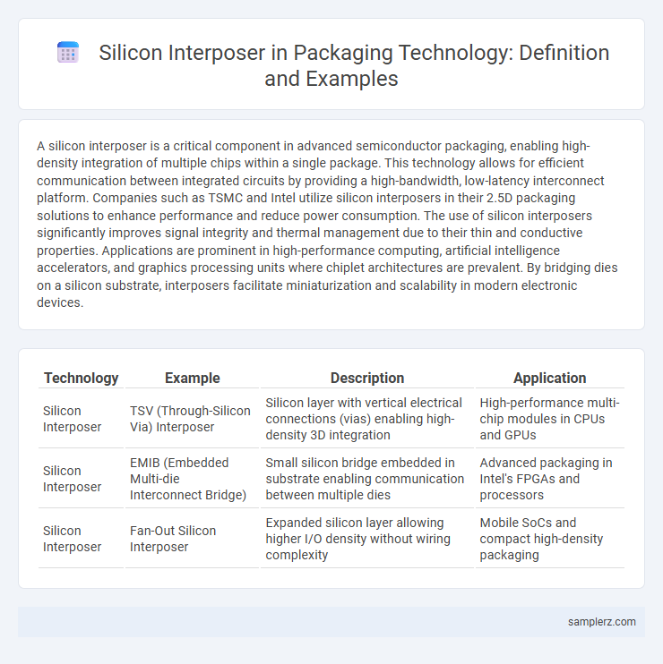
A silicon interposer is a critical component in advanced semiconductor packaging, enabling high-density integration of multiple chips within a single package. This technology allows for efficient communication between integrated circuits by providing a high-bandwidth, low-latency interconnect platform. Companies such as TSMC and Intel utilize silicon interposers in their 2.5D packaging solutions to enhance performance and reduce power consumption. The use of silicon interposers significantly improves signal integrity and thermal management due to their thin and conductive properties. Applications are prominent in high-performance computing, artificial intelligence accelerators, and graphics processing units where chiplet architectures are prevalent. By bridging dies on a silicon substrate, interposers facilitate miniaturization and scalability in modern electronic devices.
Table of Comparison
| Technology | Example | Description | Application |
|---|---|---|---|
| Silicon Interposer | TSV (Through-Silicon Via) Interposer | Silicon layer with vertical electrical connections (vias) enabling high-density 3D integration | High-performance multi-chip modules in CPUs and GPUs |
| Silicon Interposer | EMIB (Embedded Multi-die Interconnect Bridge) | Small silicon bridge embedded in substrate enabling communication between multiple dies | Advanced packaging in Intel's FPGAs and processors |
| Silicon Interposer | Fan-Out Silicon Interposer | Expanded silicon layer allowing higher I/O density without wiring complexity | Mobile SoCs and compact high-density packaging |
Introduction to Silicon Interposer Technology
Silicon interposer technology enables high-density integration by providing a thin silicon layer with through-silicon vias (TSVs) that facilitate vertical electrical connections between stacked semiconductor dies. This packaging innovation enhances performance, reduces signal delay, and improves thermal management in advanced integrated circuits for applications such as high-bandwidth memory (HBM) and heterogeneous computing systems. Leading semiconductor manufacturers use silicon interposers to achieve miniaturization and increased bandwidth in next-generation processors and memory modules.
Key Functions of Silicon Interposers in Advanced Packaging
Silicon interposers serve as critical substrates in advanced packaging, enabling high-density interconnections and efficient electrical signaling between heterogeneous components like processors and memory chips. They provide superior thermal management and signal integrity by minimizing parasitic capacitance and resistance through fine-pitch through-silicon vias (TSVs). Integration of silicon interposers supports enhanced bandwidth, reduced latency, and scalability in multi-chip modules essential for high-performance computing and AI accelerators.
Examples of Silicon Interposer Applications in High-Performance Computing
Silicon interposers are critical in high-performance computing for enabling advanced 2.5D packaging, such as in AMD's Ryzen and EPYC processors that utilize silicon interposers to connect multiple chiplets with high bandwidth and low latency. NVIDIA's HBM (High Bandwidth Memory) modules also leverage silicon interposers to integrate memory stacks closely with GPUs, significantly boosting memory bandwidth and energy efficiency. These applications demonstrate how silicon interposers provide essential pathways for signal integrity and power distribution in complex, multi-die systems.
Silicon Interposers in 2.5D Packaging Solutions
Silicon interposers serve as a critical component in 2.5D packaging by enabling high-density interconnects between multiple chiplets, significantly enhancing electrical performance and reducing latency. These ultra-thin silicon layers incorporate through-silicon vias (TSVs) that facilitate vertical signal transmission, improving bandwidth and power efficiency in complex systems like high-performance processors and advanced GPUs. Their integration supports heterogeneous integration, allowing diverse semiconductor technologies to be combined within a single package, fostering innovation in miniaturized and high-function computing devices.
Integration of HBM Memory Using Silicon Interposers
Silicon interposers enable the integration of High Bandwidth Memory (HBM) in advanced semiconductor packaging by providing a high-density interconnect platform that facilitates efficient signal routing between the processor and memory stacks. This technology enhances data transfer rates and power efficiency by minimizing the interconnect length and parasitic capacitance, critical for high-performance computing and graphics applications. Leading semiconductor manufacturers such as Intel and AMD leverage silicon interposers in their multi-chip modules to achieve superior bandwidth and reduced latency in 3D-stacked HBM configurations.
Case Study: Silicon Interposers in Graphic Processing Units (GPUs)
Silicon interposers in graphic processing units (GPUs) enhance performance by enabling high-bandwidth memory integration and efficient signal routing. For instance, AMD's Vega GPU architecture employs silicon interposers to connect High Bandwidth Memory (HBM) stacks directly to the GPU core, significantly reducing latency and power consumption. This packaging approach facilitates superior thermal management and supports increased transistor density for advanced graphics processing workloads.
Silicon Interposer Role in System-in-Package (SiP) Designs
Silicon interposers play a crucial role in System-in-Package (SiP) designs by providing a high-density interconnect platform that enables the integration of multiple heterogeneous components within a compact footprint. These interposers facilitate enhanced electrical performance and signal integrity by reducing parasitic capacitance and inductance, supporting advanced packaging techniques such as through-silicon vias (TSVs). By enabling efficient communication between processors, memory, and other functional blocks, silicon interposers significantly improve overall system performance and power efficiency in SiP solutions.
Real-World Adoption: Silicon Interposers in AI Accelerators
Silicon interposers are increasingly adopted in AI accelerators to enhance performance and power efficiency by enabling dense, high-bandwidth interconnects between compute units and memory. Companies like NVIDIA and AMD utilize silicon interposer technology in their AI chip packaging to support advanced 3D integration and heterogeneous computing architectures. This real-world application demonstrates significant improvements in data transfer speeds and thermal management, critical for large-scale AI workloads.
Benefits of Silicon Interposers for Signal Integrity and Bandwidth
Silicon interposers significantly enhance signal integrity by minimizing signal loss and crosstalk through their high-density interconnects and precise manufacturing tolerances. They support increased bandwidth by enabling shorter and more uniform signal paths, essential for high-frequency applications such as 2.5D and 3D IC packaging. These features result in improved electrical performance and efficient power distribution, making silicon interposers critical for advanced semiconductor packages.
Future Trends in Silicon Interposer Packaging Technologies
Future trends in silicon interposer packaging technologies emphasize increased integration density and enhanced thermal management to support high-performance computing and 5G applications. Advanced fabrication techniques such as through-silicon vias (TSVs) and wafer-level packaging improve signal integrity and reduce power consumption in multi-die systems. Emerging solutions also target heterogeneous integration of chips with diverse functionalities, enabling compact, scalable, and energy-efficient semiconductor devices.
example of silicon interposer in packaging Infographic