Soldermask is a protective layer applied on printed circuit boards (PCBs) to prevent solder bridges between closely spaced components. It is typically a polymer-based coating that covers the copper traces, except for the pads where components are soldered. The green soldermask is most common, but colors like blue, red, and black are also used depending on the manufacturer and application. In PCB manufacturing, soldermask enhances electrical insulation and protects against oxidation and environmental damage. It plays a critical role in enabling precise soldering by defining areas where solder should adhere, reducing the risk of short circuits. Electronic devices such as smartphones, computers, and automotive control systems rely heavily on PCBs with high-quality soldermasks for reliable performance.
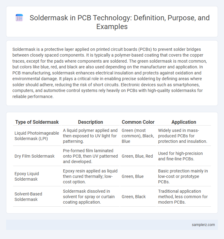
Table of Comparison
| Type of Soldermask | Description | Common Color | Application |
|---|---|---|---|
| Liquid Photoimageable Soldermask (LPI) | A liquid polymer applied and then exposed to UV light for patterning. | Green (most common), Black, Blue | Widely used in mass-produced PCBs for protection and insulation. |
| Dry Film Soldermask | Pre-formed film laminated onto PCB, then UV patterned and developed. | Green, Blue, Red | Used for high-precision and fine-line PCBs. |
| Epoxy Liquid Soldermask | Epoxy resin applied as liquid then cured thermally; low-cost option. | Green, Blue | Basic protection mainly in low-cost or prototype PCBs. |
| Solvent-Based Soldermask | Soldermask dissolved in solvent for spray or curtain coating application. | Green, Black | Traditional application method, less common for modern PCBs. |
Understanding Soldermask in PCB Manufacturing
Soldermask in PCB manufacturing serves as a protective layer that insulates copper traces, preventing short circuits and corrosion while ensuring reliable soldering during assembly. Common examples include green epoxy-based soldermask, which offers excellent adhesion and thermal resistance, and blue or black soldermasks used for aesthetic or functional differentiation. Proper application and curing of soldermask enhance PCB durability, electrical performance, and manufacturability by maintaining precise circuit patterns and protecting against environmental contaminants.
Types of Soldermask Used in PCBs
Soldermask types used in PCBs include liquid photoimageable soldermask (LPI), dry film soldermask, and liquid screen-printable soldermask, each offering distinct advantages in application methods and resolution. LPI soldermask is the most common, providing excellent fine-line resolution and flexibility for complex PCB designs. Dry film soldermask offers superior thickness control and is preferred for high-volume production, while liquid screen-printable soldermask is cost-effective for simple, low-volume boards.
Common Examples of Soldermask Materials
Common examples of soldermask materials in PCB manufacturing include epoxy liquid, liquid photoimageable soldermask (LPSM), and dry film soldermask. Epoxy liquid offers cost-effectiveness and basic protection, while LPSM provides higher resolution and is widely used for complex, fine-pitch PCBs. Dry film soldermask delivers excellent uniformity and thickness control, making it ideal for multilayer circuit boards and high-density designs.
Soldermask Application Techniques in PCB Fabrication
Soldermask application techniques in PCB fabrication include screen printing, curtain coating, and photoimageable soldermask processes, each ensuring precise coverage to prevent solder bridges. Screen printing deposits soldermask through a mesh stencil, suitable for standard boards, while curtain coating flows soldermask evenly across complex surfaces. Photoimageable soldermask utilizes UV light to harden selective areas, offering high-resolution patterns essential for fine-pitch components and advanced PCB designs.
Popular Soldermask Colors and Their Uses
Green soldermask remains the most popular choice in PCB manufacturing due to its excellent contrast with copper traces, aiding in inspection and repair. Black soldermask is favored for high-end consumer electronics, offering a sleek aesthetic while providing good insulation and resistance to environmental factors. Blue and red soldermasks are often used for specialized or prototype boards, enhancing visual differentiation during testing phases and design validation.
Case Study: Soldermask Selection in High-Density PCBs
Soldermask selection in high-density PCBs critically impacts circuit reliability and manufacturing yield by preventing solder bridging and ensuring precise pad definition. Case studies demonstrate that using liquid photoimageable soldermask materials enhances resolution and adhesion on fine-pitch components, reducing defects in complex multilayer boards. Advanced formulations with high thermal stability and low dielectric constants support improved signal integrity and enable miniaturization in high-frequency applications.
Soldermask vs. Other PCB Protective Coatings
Soldermask is a critical protective layer on PCBs that prevents solder bridges and corrosion during assembly, enhancing circuit reliability compared to other coatings like conformal coatings or epoxy. Unlike conformal coatings, soldermask allows precise exposure of pads for soldering while providing excellent electrical insulation and chemical resistance. Its widespread use in modern electronics manufacturing is due to its cost-effectiveness, durability, and ability to improve manufacturing yield by reducing defects.
Industry Standards for PCB Soldermask
Industry standards for PCB soldermask, such as IPC-SM-840 and IPC-4552, define the chemical composition, thickness, and adhesion properties required to ensure reliable insulation and protection against environmental factors. These standards also specify parameters for soldermask registration accuracy and coverage to prevent solder bridging during the assembly process. Compliance with these guidelines is critical for enhancing PCB durability, electrical insulation, and overall manufacturing yield.
Troubleshooting Soldermask Issues in PCB Production
Soldermask defects in PCB production often include issues such as inadequate coverage, peeling, or contamination, which can lead to short circuits or poor solder joint quality. Troubleshooting these problems involves verifying the proper application thickness, ensuring the curing process reaches the specified temperature, and inspecting PCB surface cleanliness before mask application. Utilizing automated optical inspection (AOI) systems enhances defect detection, enabling early correction and minimizing PCB rework costs.
Innovations in Soldermask Technology for Modern Electronics
Advanced soldermask formulations in PCB manufacturing now feature enhanced thermal resistance and improved chemical durability, enabling higher-frequency signal integrity in modern electronics. Innovations include UV-curable soldermasks with precise layer control that reduce defects during assembly, supporting miniaturized and high-density circuit designs. Emerging materials with better adhesion and environmental stability contribute to longer PCB lifespan and reliable performance in harsh operating conditions.
example of soldermask in PCB Infographic