Photolithography is a critical process in semiconductor manufacturing used to transfer intricate circuit patterns onto silicon wafers. This technique involves coating the wafer with a light-sensitive photoresist, exposing it to ultraviolet light through a mask, and then developing the image to create precise geometric shapes. These patterns define the locations of transistors, interconnects, and other microscopic components essential for integrated circuits. Semiconductor fabrication plants utilize advanced photolithography systems employing deep ultraviolet (DUV) and extreme ultraviolet (EUV) light sources to achieve feature sizes as small as a few nanometers. Companies like ASML dominate the market by providing cutting-edge photolithography machines that enable high-resolution patterning necessary for modern processors and memory chips. The precise control of photolithography parameters directly impacts device performance, yield, and scalability in the semiconductor industry.
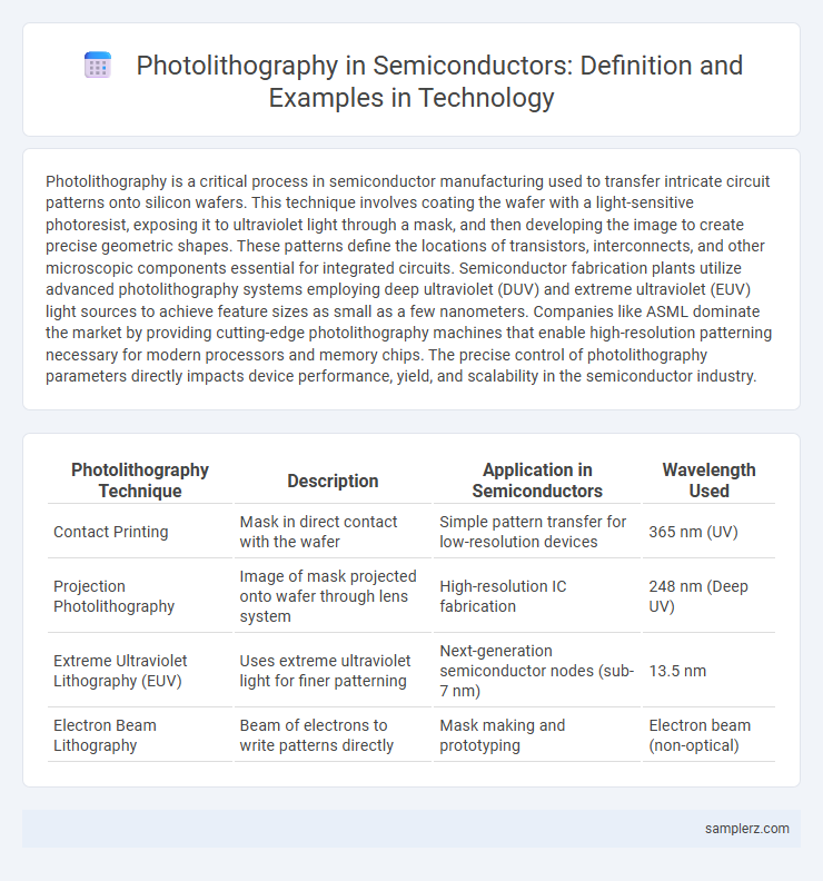
Table of Comparison
| Photolithography Technique | Description | Application in Semiconductors | Wavelength Used |
|---|---|---|---|
| Contact Printing | Mask in direct contact with the wafer | Simple pattern transfer for low-resolution devices | 365 nm (UV) |
| Projection Photolithography | Image of mask projected onto wafer through lens system | High-resolution IC fabrication | 248 nm (Deep UV) |
| Extreme Ultraviolet Lithography (EUV) | Uses extreme ultraviolet light for finer patterning | Next-generation semiconductor nodes (sub-7 nm) | 13.5 nm |
| Electron Beam Lithography | Beam of electrons to write patterns directly | Mask making and prototyping | Electron beam (non-optical) |
Introduction to Photolithography in Semiconductor Manufacturing
Photolithography is a critical process in semiconductor manufacturing that uses light to transfer a geometric pattern from a photomask to a light-sensitive chemical photoresist on the substrate. This patterning technique enables the creation of intricate circuit designs on silicon wafers, forming the foundation for integrated circuits and microchips. Advanced photolithography methods, such as deep ultraviolet (DUV) and extreme ultraviolet (EUV) lithography, drive the production of smaller, faster, and more efficient semiconductor devices.
Key Principles of Photolithography Technology
Photolithography technology in semiconductors relies on the precise transfer of circuit patterns onto silicon wafers using ultraviolet (UV) light through a photomask. Key principles include the use of photosensitive photoresist materials that chemically alter when exposed to light, enabling selective etching or doping of the wafer surface. This process hinges on factors like wavelength, resolution limits, and alignment accuracy to achieve intricate micro-scale features essential for integrated circuit fabrication.
Historical Evolution of Photolithography Techniques
Photolithography techniques in semiconductor manufacturing evolved from contact printing in the 1950s to advanced projection methods using deep ultraviolet (DUV) and extreme ultraviolet (EUV) lithography in the 21st century. The transition to photomasks and stepper tools significantly improved pattern resolution and alignment accuracy, enabling the production of integrated circuits with feature sizes below 100 nanometers. Continuous innovations such as immersion lithography and multiple patterning have pushed the boundaries further, supporting the demand for smaller transistors and higher chip performance in modern microprocessors.
Photolithography Process Steps in Chip Fabrication
Photolithography in semiconductor chip fabrication involves several critical steps, starting with coating the silicon wafer with a light-sensitive photoresist layer. The coated wafer is then exposed to ultraviolet light through a photomask that defines the circuit pattern. Following exposure, the wafer undergoes a development process where the exposed or unexposed photoresist is removed, allowing subsequent etching or doping to precisely form the intricate transistor structures on the chip.
Deep Ultraviolet (DUV) Photolithography Applications
Deep Ultraviolet (DUV) photolithography plays a critical role in semiconductor manufacturing by enabling the patterning of intricate circuit designs on silicon wafers at wavelengths typically around 248 nm and 193 nm. This technology is essential for producing microchips with feature sizes down to 65 nanometers, supporting high-performance processors and memory devices. DUV photolithography's ability to deliver high resolution and throughput makes it a cornerstone in the fabrication of advanced integrated circuits used in smartphones, computers, and automotive electronics.
Extreme Ultraviolet (EUV) Photolithography in Modern Semiconductors
Extreme Ultraviolet (EUV) photolithography uses 13.5 nm wavelength light to pattern intricate features on semiconductor wafers, enabling the production of advanced integrated circuits with nodes below 7 nm. This technology significantly enhances transistor density, performance, and power efficiency compared to deep ultraviolet (DUV) lithography. Key semiconductor manufacturers like TSMC and Samsung rely on EUV lithography for mass production of cutting-edge chips used in smartphones, AI, and high-performance computing.
Real-World Example: Photolithography in Logic Chip Production
Photolithography is crucial in manufacturing advanced logic chips like Intel's 7nm processors, enabling precise patterning of transistors on silicon wafers. Using extreme ultraviolet (EUV) lithography, intricate circuitry with features smaller than 10 nanometers is achieved, enhancing performance and energy efficiency. This process underpins the production of high-speed, low-power microprocessors essential for modern computing devices.
Photolithography Role in Memory Device Fabrication
Photolithography plays a critical role in memory device fabrication by enabling the precise patterning of intricate circuit features on silicon wafers. This technology allows for the creation of nanoscale structures essential for DRAM and NAND flash memory cells, directly influencing device density and performance. Advanced photolithography techniques such as extreme ultraviolet (EUV) lithography improve resolution and throughput, driving advancements in high-capacity memory chip production.
Challenges and Limitations in Photolithography for Semiconductors
Photolithography in semiconductor manufacturing faces critical challenges such as resolution limits imposed by the wavelength of light, which restricts feature miniaturization beyond certain nanometer scales. Process variability and defects stem from issues like photoresist sensitivity and alignment precision, affecting yield and device performance. High equipment costs and complex chemical processes further constrain scalability and innovation in advanced node production.
Future Trends in Photolithography for Advanced Electronics
Next-generation photolithography techniques, such as extreme ultraviolet (EUV) and nanoimprint lithography, are driving the miniaturization of semiconductor devices beyond the 3-nanometer node. Innovations in multipatterning and directed self-assembly are enhancing pattern resolution and throughput for advanced integrated circuits. Machine learning algorithms optimize mask design and process control, accelerating development cycles in advanced electronics manufacturing.
example of photolithography in semiconductor Infographic