Die-stacking in microprocessors is a cutting-edge technique that involves vertically stacking multiple silicon dies to enhance performance and reduce power consumption. One prominent example is the High Bandwidth Memory (HBM) used in AMD's Ryzen processors, where memory dies are stacked on top of a logic die to increase data transfer speeds. This architecture allows for a shorter interconnect distance, leading to faster communication between the cores and memory units. Another notable instance of die-stacking is seen in Intel's Foveros technology, which integrates logic dies and memory dies in a 3D configuration. This technology is used in the Intel Lakefield processors, combining high-performance and low-power cores within a single package. The 3D die stacking approach significantly improves energy efficiency and chip scalability in modern microprocessors.
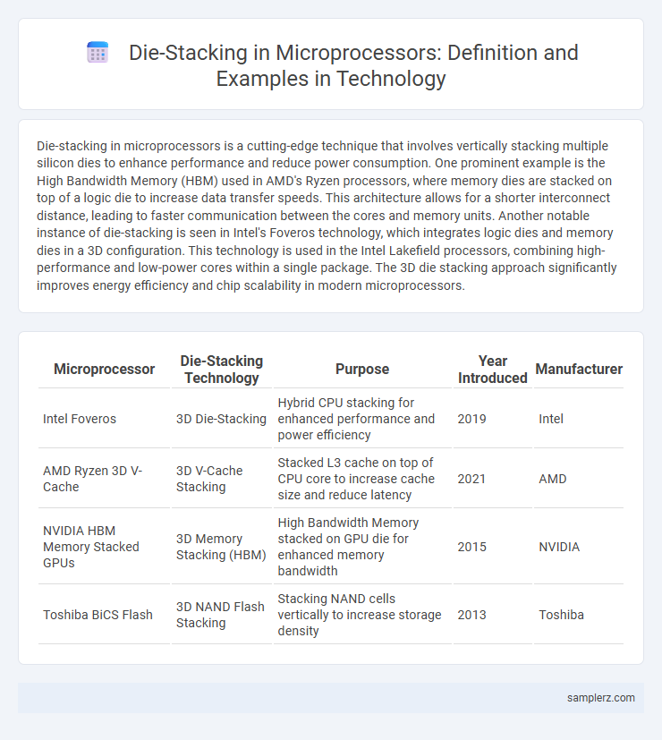
Table of Comparison
| Microprocessor | Die-Stacking Technology | Purpose | Year Introduced | Manufacturer |
|---|---|---|---|---|
| Intel Foveros | 3D Die-Stacking | Hybrid CPU stacking for enhanced performance and power efficiency | 2019 | Intel |
| AMD Ryzen 3D V-Cache | 3D V-Cache Stacking | Stacked L3 cache on top of CPU core to increase cache size and reduce latency | 2021 | AMD |
| NVIDIA HBM Memory Stacked GPUs | 3D Memory Stacking (HBM) | High Bandwidth Memory stacked on GPU die for enhanced memory bandwidth | 2015 | NVIDIA |
| Toshiba BiCS Flash | 3D NAND Flash Stacking | Stacking NAND cells vertically to increase storage density | 2013 | Toshiba |
Introduction to Die-Stacking Technology in Microprocessors
Die-stacking technology in microprocessors involves vertically layering multiple semiconductor dies to enhance performance and reduce latency by increasing interconnect density. This method enables integration of logic and memory components within a compact footprint, significantly improving data bandwidth and energy efficiency. Prominent examples include Intel's Foveros and AMD's 3D V-Cache architectures, which leverage die-stacking to boost computational power in modern processors.
Historical Milestones of Die-Stacking in CPU Design
Die-stacking technology in microprocessor design began with IBM's 2001 introduction of the POWER4 CPU, which integrated two dies in a single package to improve performance and reduce latency. Intel advanced the concept with its 2016 development of 3D Tri-Gate transistors and Foveros packaging, enabling heterogeneous die integration for enhanced power efficiency. Recent milestones include AMD's use of chiplet architecture in its Ryzen processors, leveraging die-stacking to optimize scalability and manufacturing yields.
How Die-Stacking Enhances Microprocessor Performance
Die-stacking in microprocessors involves vertically integrating multiple silicon dies to enhance computing efficiency by reducing interconnect distances and increasing bandwidth between cores and memory. This architecture significantly lowers latency and power consumption, enabling faster data transfer and improved thermal management compared to traditional planar designs. Technologies like Intel's Foveros and TSMC's Chip-on-Wafer-on-Substrate (CoWoS) demonstrate how die-stacking optimizes parallel processing capabilities and overall system performance in advanced CPUs.
2.5D vs 3D Die-Stacking: Key Differences and Applications
2.5D die-stacking integrates multiple silicon dies side-by-side on an interposer, enabling high-bandwidth interconnects with easier heat dissipation, commonly used in advanced GPUs and AI accelerators. 3D die-stacking vertically stacks dies with through-silicon vias (TSVs), offering greater density and lower latency, ideal for memory integration like High Bandwidth Memory (HBM) in microprocessors. The choice between 2.5D and 3D impacts power efficiency, thermal management, and performance scaling in multi-die microprocessor architectures.
Real-World Examples of Die-Stacking in Modern Processors
High Bandwidth Memory (HBM) integrated with AMD's Ryzen processors showcases die-stacking by vertically stacking DRAM dies to achieve faster data transfer rates and reduced latency. Intel's Foveros 3D packaging technology in their Lakefield processors stacks CPU cores atop a base die, optimizing power efficiency and performance in compact devices. NVIDIA's use of die-stacking in their GPU HBM modules enables significant improvements in memory bandwidth critical for AI and graphics workloads.
AMD’s Use of Die-Stacking: Ryzen and EPYC Case Studies
AMD employs die-stacking technology in its Ryzen and EPYC processors to enhance performance and energy efficiency by integrating multiple silicon dies within a single package. The Ryzen series utilizes 3D chiplet integration to increase core counts and optimize interconnect bandwidth, while EPYC processors leverage die-stacking to scale memory channels and boost server workloads. This approach enables AMD to deliver higher computational throughput and improved thermal management compared to traditional monolithic designs.
Intel’s Foveros Technology: A Die-Stacking Breakthrough
Intel's Foveros technology exemplifies advanced die-stacking by vertically integrating multiple active silicon layers within a single microprocessor package, dramatically enhancing performance and power efficiency. This 3D packaging approach enables heterogeneous integration of different process nodes, allowing high-bandwidth memory and specialized compute units to coexist closely. Foveros improves thermal management and reduces interconnect latency, marking a significant breakthrough in modern microprocessor design.
Thermal Management Challenges in Stacked Microprocessors
Die-stacking in microprocessors, such as Intel's Foveros technology, presents significant thermal management challenges due to increased power density and reduced heat dissipation pathways. Efficient heat spreaders and advanced cooling solutions like microfluidic channels become crucial to mitigate hotspots and maintain performance stability. Thermal interface materials with high conductivity also play a key role in managing the thermal resistance between stacked dies.
Future Trends: Die-Stacking in AI and High-Performance Computing
Die-stacking technology enables enhanced performance and energy efficiency in AI and high-performance computing by vertically integrating multiple layers of logic and memory on a single chip, exemplified by AMD's 3D V-Cache and Intel's Foveros packaging. Future trends highlight increased adoption of heterogeneous integration, combining specialized AI accelerators, high-bandwidth memory, and advanced interconnects to overcome latency and bandwidth bottlenecks. This progression supports scalable architectures crucial for machine learning workloads and exascale computing systems.
Impact of Die-Stacking on Energy Efficiency and Miniaturization
Die-stacking technology in microprocessors significantly enhances energy efficiency by reducing the distance data must travel between stacked dies, thereby lowering power consumption and heat generation. This vertical integration facilitates greater transistor density on a smaller footprint, driving advanced miniaturization and improved performance of semiconductor devices. Innovations such as High Bandwidth Memory (HBM) stacks exemplify how die-stacking optimizes bandwidth while minimizing latency, crucial for energy-conscious, compact electronic systems.
example of die-stacking in microprocessor Infographic