Photonic crystals are materials with periodic variations in refractive index that affect the propagation of light. An example of a photonic crystal used in waveguides is the silicon-based photonic crystal slab waveguide, which confines and guides light within a two-dimensional periodic structure. These waveguides leverage the photonic bandgap property of the crystal to control light propagation with high precision and low loss. In integrated optics, photonic crystal waveguides are essential for routing optical signals on chips with minimal cross-talk and dispersion. The periodic air holes etched into silicon form the photonic crystal pattern that enables efficient waveguiding by creating forbidden frequency bands for light outside the guidance mode. This technology is critical for developing compact, high-performance optical communication and sensing devices.
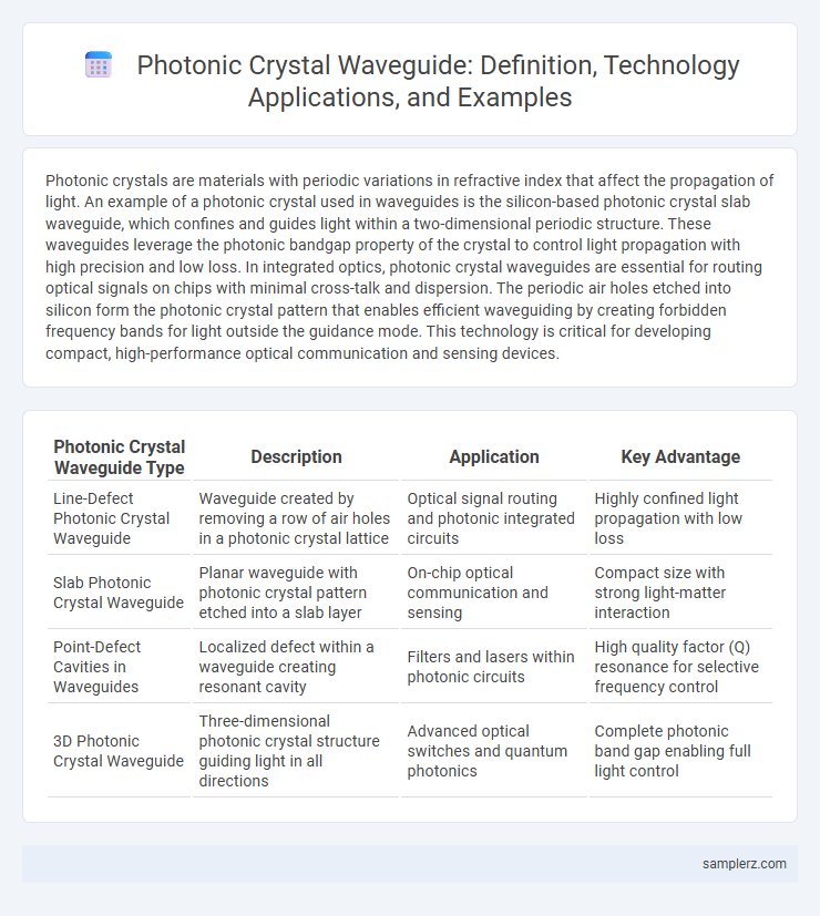
Table of Comparison
| Photonic Crystal Waveguide Type | Description | Application | Key Advantage |
|---|---|---|---|
| Line-Defect Photonic Crystal Waveguide | Waveguide created by removing a row of air holes in a photonic crystal lattice | Optical signal routing and photonic integrated circuits | Highly confined light propagation with low loss |
| Slab Photonic Crystal Waveguide | Planar waveguide with photonic crystal pattern etched into a slab layer | On-chip optical communication and sensing | Compact size with strong light-matter interaction |
| Point-Defect Cavities in Waveguides | Localized defect within a waveguide creating resonant cavity | Filters and lasers within photonic circuits | High quality factor (Q) resonance for selective frequency control |
| 3D Photonic Crystal Waveguide | Three-dimensional photonic crystal structure guiding light in all directions | Advanced optical switches and quantum photonics | Complete photonic band gap enabling full light control |
Introduction to Photonic Crystals in Waveguides
Photonic crystals in waveguides manipulate light propagation by creating periodic dielectric structures that produce photonic band gaps, effectively controlling electromagnetic wave transmission. This technology enhances the performance of optical waveguides by minimizing losses and enabling precise light confinement within nanoscale dimensions. Applications include improving integrated optical circuits, sensors, and telecommunications systems through efficient light routing and filtering.
Key Principles of Photonic Crystal Waveguides
Photonic crystal waveguides manipulate light by creating periodic dielectric structures that produce photonic band gaps, effectively controlling photon propagation. These waveguides utilize defects or channels within the crystal lattice to confine and guide light with minimal loss, enabling precise control over wavelength and mode dispersion. The key principles include strong light confinement through Bragg scattering and tailored dispersion properties, which make photonic crystal waveguides essential for advanced optical communication and integrated photonic circuits.
Types of Photonic Crystal Waveguide Structures
Photonic crystal waveguide structures include line-defect waveguides, where a single row of holes is removed to guide light through a photonic bandgap, and coupled-cavity waveguides formed by an array of coupled resonators enabling slow light propagation. Slot waveguides utilize a narrow low-index region between two high-index photonic crystal slabs to confine and enhance optical fields. These types optimize light manipulation for applications in optical communication and integrated photonic circuits.
Design and Fabrication of Photonic Crystal Waveguides
Photonic crystal waveguides are engineered by introducing line defects within a periodic lattice of dielectric materials, enabling precise control of light propagation through photonic bandgap effects. Fabrication techniques such as electron beam lithography and reactive ion etching are commonly employed to achieve nanoscale precision and high structural quality necessary for optimal waveguide performance. Advanced designs incorporate optimized lattice constants and defect geometries to minimize losses and enhance confinement in integrated photonic circuits.
Photonic Bandgap Effects in Waveguides
Photonic crystals in waveguides exploit photonic bandgap effects to control light propagation by creating frequency ranges where electromagnetic waves cannot travel, enabling highly efficient light confinement and guiding. These bandgap effects result from the periodic dielectric structure, which inhibits certain wavelengths, enhancing the performance of optical circuits and sensors. Waveguides incorporating photonic crystals show improved dispersion management and reduced optical losses, critical for next-generation photonic devices.
Real-World Examples of Photonic Crystal Waveguides
Photonic crystal waveguides, such as those used in silicon photonics, enable precise control of light propagation for optical communication systems. Real-world applications include on-chip optical interconnects that enhance data transmission speeds while reducing energy consumption in data centers. Companies like Intel and IBM utilize photonic crystal waveguides to improve performance in integrated photonic circuits.
Applications of Photonic Crystal Waveguide Technologies
Photonic crystal waveguides enable precise control of light propagation, crucial for integrated optical circuits and on-chip communication systems. These waveguides enhance performance in optical sensors by improving sensitivity and enabling miniaturization for lab-on-chip devices. Applications extend to quantum computing and nonlinear optics, where photonic crystals facilitate low-loss light confinement and manipulation at the nanoscale.
Advantages of Photonic Crystal Waveguides Over Traditional Waveguides
Photonic crystal waveguides offer superior light confinement and reduced scattering losses compared to traditional waveguides, enabling ultra-compact photonic circuits with enhanced performance. Their ability to engineer photonic band gaps allows precise control over light propagation, resulting in lower signal distortion and increased bandwidth. These advantages make photonic crystal waveguides ideal for high-speed optical communication and integrated photonics applications.
Challenges in Implementing Photonic Crystal Waveguides
Fabricating photonic crystal waveguides demands nanoscale precision to achieve the required periodicity for effective light confinement, posing significant manufacturing challenges. Material imperfections and surface roughness introduce scattering losses that degrade waveguide performance and limit device efficiency. Integration with existing photonic circuits requires overcoming compatibility issues between photonic crystals and conventional waveguide materials, complicating scalable production.
Future Trends in Photonic Crystal Waveguide Research
Emerging research in photonic crystal waveguides emphasizes the integration of topological photonics to enhance robustness against defects and scattering losses. Advancements in nanoscale fabrication techniques are enabling unprecedented control over light-matter interaction, leading to ultra-compact and efficient optical circuits. Exploration of novel materials such as silicon carbide and two-dimensional materials is driving progress toward tunable and reconfigurable photonic crystal waveguides for next-generation communication systems.
example of photonic crystal in waveguide Infographic