Photolithography plays a crucial role in semiconductor manufacturing, enabling the precise patterning of circuits on silicon wafers. This technology uses light to transfer geometric patterns from photomasks onto a photosensitive chemical photoresist layer. Companies like Intel and TSMC utilize advanced photolithography techniques to produce integrated circuits with feature sizes as small as 3 nanometers. The data generated from photolithography processes directly impacts chip performance, yield, and reliability. Measurements such as critical dimension uniformity and overlay accuracy help optimize the process for higher-quality chips. In recent years, extreme ultraviolet (EUV) lithography has emerged as a key innovation, improving resolution and supporting the production of cutting-edge microprocessors and memory devices.
Table of Comparison
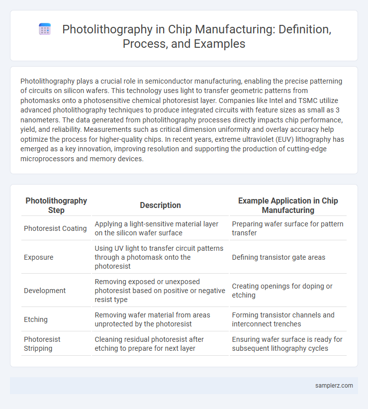
| Photolithography Step | Description | Example Application in Chip Manufacturing |
|---|---|---|
| Photoresist Coating | Applying a light-sensitive material layer on the silicon wafer surface | Preparing wafer surface for pattern transfer |
| Exposure | Using UV light to transfer circuit patterns through a photomask onto the photoresist | Defining transistor gate areas |
| Development | Removing exposed or unexposed photoresist based on positive or negative resist type | Creating openings for doping or etching |
| Etching | Removing wafer material from areas unprotected by the photoresist | Forming transistor channels and interconnect trenches |
| Photoresist Stripping | Cleaning residual photoresist after etching to prepare for next layer | Ensuring wafer surface is ready for subsequent lithography cycles |
Introduction to Photolithography in Chip Manufacturing
Photolithography in chip manufacturing involves transferring intricate circuit patterns onto silicon wafers using light-sensitive photoresist materials and precise UV light exposure. This technology enables the production of micro-scale features essential for integrated circuits, ensuring high resolution and accuracy in semiconductor devices. Advanced photolithography techniques, such as extreme ultraviolet (EUV) lithography, significantly improve chip performance by allowing smaller transistor sizes and higher density integration.
Key Steps of Photolithography Process in Semiconductors
Photolithography in semiconductor manufacturing involves key steps such as coating the silicon wafer with a photoresist, exposing it to ultraviolet light through a photomask to transfer circuit patterns, and developing the exposed photoresist to create a precise etch-resistant layer. Subsequent etching processes remove unwanted material, enabling the formation of microscale transistors essential for integrated circuits. Advanced photolithography techniques, including deep ultraviolet (DUV) and extreme ultraviolet (EUV) lithography, push the limits of feature size reduction in modern microchip fabrication.
Types of Photolithography Techniques Used in Chip Fabrication
Photolithography techniques in chip fabrication include contact, proximity, and projection lithography, each differing in mask-to-wafer distance and resolution capabilities. Projection lithography, especially deep ultraviolet (DUV) and extreme ultraviolet (EUV), enables high-precision patterning essential for advanced semiconductor nodes. Electron beam lithography (EBL) offers maskless direct writing, ideal for prototyping and niche applications requiring nanometer-scale feature sizes.
Role of Photoresist Materials in Integrated Circuits
Photoresist materials play a critical role in photolithography by enabling precise pattern transfer onto semiconductor wafers, essential for fabricating integrated circuits. These light-sensitive polymers undergo chemical changes when exposed to ultraviolet light, allowing selective removal during development to create intricate circuit designs. Advances in photoresist chemistry improve resolution, sensitivity, and etch resistance, directly impacting the performance and miniaturization of modern microchips.
Example: Patterning Transistor Gates with Photolithography
Photolithography is crucial in patterning transistor gates by using UV light to transfer circuit designs onto silicon wafers with extreme precision. This technique enables the creation of nanoscale features essential for defining gate lengths that directly impact transistor performance and power efficiency. Advances in photolithography, such as extreme ultraviolet (EUV) lithography, have further enhanced resolution, supporting the production of smaller, faster, and more energy-efficient semiconductor devices.
Deep Ultraviolet (DUV) Lithography in Advanced Chips
Deep Ultraviolet (DUV) lithography employs wavelengths typically around 193 nm to create intricate patterns on semiconductor wafers, enabling the production of advanced chips with feature sizes below 10 nanometers. This technology supports high-throughput manufacturing and precise layer alignment crucial for modern processors and memory devices. DUV lithography remains a cost-effective solution for mass production of integrated circuits, particularly in logic and DRAM chips.
Extreme Ultraviolet (EUV) Lithography: A Modern Breakthrough
Extreme Ultraviolet (EUV) Lithography revolutionizes semiconductor manufacturing by utilizing 13.5 nm wavelength light to etch intricate patterns on silicon wafers, enabling the production of chips with features smaller than 7 nanometers. Semiconductor giants like ASML lead the development of EUV machines, which improve precision and throughput compared to traditional photolithography techniques. This breakthrough accelerates advancements in processors, memory devices, and integrated circuits, pushing the limits of Moore's Law.
Challenges in Photolithography for Miniaturized Chips
Photolithography faces critical challenges in producing miniaturized chips, especially as feature sizes approach the nanometer scale, demanding extreme ultraviolet (EUV) light sources with wavelengths below 14nm. Issues such as light diffraction limits, resist sensitivity, and pattern distortions increase, requiring advanced mask alignments and precise overlay controls. High costs and complexity in equipment also pose significant barriers to scaling photolithography for next-generation semiconductor manufacturing.
Photolithography Equipment Used in Chip Production
Photolithography equipment such as steppers and scanners play a crucial role in defining intricate circuit patterns on silicon wafers during chip production. Deep ultraviolet (DUV) and extreme ultraviolet (EUV) lithography systems enable semiconductor manufacturers like ASML to achieve nanometer-scale resolution essential for advanced microprocessors and memory chips. Precise alignment and exposure control in photolithography tools directly impact the yield, performance, and scaling of integrated circuits in modern technology.
Future Trends in Photolithography for Microprocessors
Future trends in photolithography for microprocessors emphasize extreme ultraviolet (EUV) lithography, enabling feature sizes below 5 nanometers, which enhances transistor density and performance. Advances in multiple patterning techniques and next-generation resist materials will improve resolution and minimize defects during chip fabrication. Integration of AI-driven process control and in-situ metrology promises higher precision and yield optimization in semiconductor manufacturing.
example of photolithography in chip Infographic