Nanoribbons are ultra-thin strips of material, often just a few atoms wide, used in the fabrication of transistors to enhance performance and miniaturization. Graphene nanoribbons, for instance, exhibit exceptional electrical conductivity and tunable bandgaps, making them ideal candidates for next-generation transistors. These structures offer significant advantages in reducing power consumption and increasing switching speeds compared to traditional silicon-based components. Semiconductor nanoribbons made from materials such as molybdenum disulfide (MoS2) demonstrate remarkable semiconducting properties and scalability in transistor applications. The use of MoS2 nanoribbons in field-effect transistors (FETs) enables high on/off current ratios and excellent electrostatic control. Research continues to focus on optimizing the synthesis and integration of nanoribbons to improve transistor efficiency and functionality at the nanoscale.
Table of Comparison
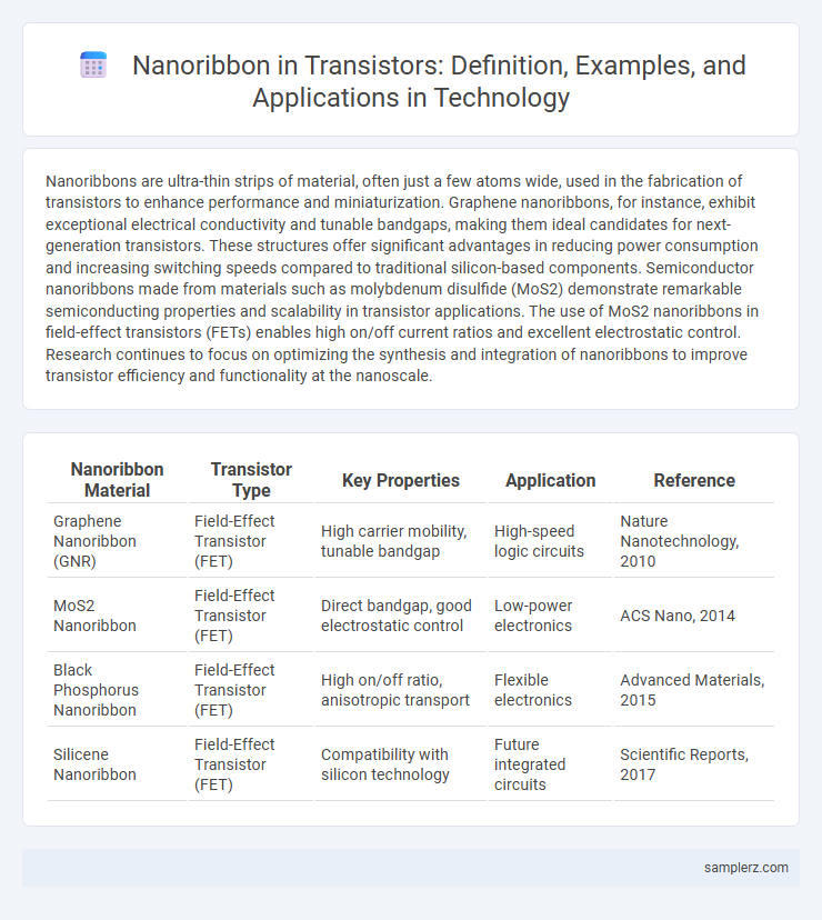
| Nanoribbon Material | Transistor Type | Key Properties | Application | Reference |
|---|---|---|---|---|
| Graphene Nanoribbon (GNR) | Field-Effect Transistor (FET) | High carrier mobility, tunable bandgap | High-speed logic circuits | Nature Nanotechnology, 2010 |
| MoS2 Nanoribbon | Field-Effect Transistor (FET) | Direct bandgap, good electrostatic control | Low-power electronics | ACS Nano, 2014 |
| Black Phosphorus Nanoribbon | Field-Effect Transistor (FET) | High on/off ratio, anisotropic transport | Flexible electronics | Advanced Materials, 2015 |
| Silicene Nanoribbon | Field-Effect Transistor (FET) | Compatibility with silicon technology | Future integrated circuits | Scientific Reports, 2017 |
Introduction to Nanoribbons in Transistor Technology
Nanoribbons serve as key components in transistor technology due to their exceptional electrical conductivity and quantum confinement effects, enabling enhanced performance at nanoscale dimensions. Graphene nanoribbons, in particular, exhibit tunable bandgaps that improve transistor switching capabilities and reduce power consumption. Integration of these nanoribbons into field-effect transistors (FETs) facilitates miniaturization while maintaining high carrier mobility and stability.
Key Properties of Nanoribbons for Transistor Applications
Nanoribbons exhibit exceptional electrical conductivity and high carrier mobility, making them ideal for transistor applications. Their atomically thin structure enables excellent gate control and reduced short-channel effects, crucial for scaling down transistor sizes. Enhanced surface-to-volume ratio in nanoribbons also improves sensitivity and performance in next-generation nanoscale transistors.
Graphene Nanoribbons: Pioneering Examples in Transistors
Graphene nanoribbons (GNRs) exhibit exceptional electrical properties, making them ideal for next-generation transistor channels due to their tunable bandgap and high carrier mobility. Key examples include GNR-based field-effect transistors (FETs) that demonstrate enhanced switching behavior and low power consumption compared to traditional silicon transistors. Experimental studies highlight GNR transistors operating at nanoscale dimensions, showcasing their potential in ultra-fast, energy-efficient electronics and flexible device applications.
Silicon Nanoribbons in Next-Generation FETs
Silicon nanoribbons exhibit exceptional electrical properties that enable enhanced carrier mobility and reduced power consumption in next-generation field-effect transistors (FETs). Their ultra-thin structure allows for effective channel control, minimizing short-channel effects and improving device scalability at sub-5nm technology nodes. Integration of silicon nanoribbons in FET architectures promises significant advancements in high-performance computing and low-power electronics.
Transition Metal Dichalcogenide (TMD) Nanoribbon Transistors
Transition Metal Dichalcogenide (TMD) nanoribbon transistors exhibit exceptional electrical properties due to their atomically thin structure and tunable bandgap, making them ideal for next-generation nanoelectronic devices. Materials like MoS2 and WS2 nanoribbons provide high carrier mobility and excellent gate control, enabling low-power, high-performance transistor applications. Their quantum confinement effects and strong spin-orbit coupling further enhance device scalability and functional diversity in integrated circuits.
Fabrication Techniques of Nanoribbon-Based Transistors
Fabrication techniques of nanoribbon-based transistors leverage advanced lithography and etching methods to achieve precise control over ribbon width and thickness, essential for optimizing electronic properties. Chemical vapor deposition (CVD) and molecular beam epitaxy (MBE) are commonly employed for high-quality nanoribbon synthesis, ensuring uniformity and minimal defects. Atomic layer deposition (ALD) further enhances gate dielectric layers, crucial for improving transistor performance and scalability in next-generation nanoelectronic devices.
Performance Comparisons: Nanoribbon vs Conventional Channel Materials
Nanoribbon transistors exhibit superior electron mobility and reduced short-channel effects compared to conventional silicon channel materials, enhancing device speed and energy efficiency. Their atomically thin structure allows for better electrostatic control, minimizing leakage currents and enabling higher integration densities. Performance benchmarks reveal that nanoribbon-based devices outperform traditional planar transistors in switching speed and power consumption, making them promising candidates for next-generation nanoelectronics.
Real-World Applications of Nanoribbon Transistors
Nanoribbon transistors enable ultra-scaled, high-performance electronics by offering exceptional electrical control and reduced short-channel effects. Real-world applications include flexible displays, where nanoribbon transistors provide enhanced mechanical flexibility and energy efficiency, and advanced sensors in Internet of Things (IoT) devices, benefiting from their high sensitivity and low power consumption. Integration of nanoribbon transistors in next-generation microprocessors promises significant improvements in speed and thermal management.
Challenges in Integrating Nanoribbons into Modern Circuits
Integrating nanoribbons into modern transistors faces challenges such as controlling their precise width and edge structure to ensure consistent electrical properties. Fabrication techniques must address defects and variability at the nanoscale, which impact device reliability and performance. Scaling nanoribbon-based transistors while maintaining compatibility with existing semiconductor manufacturing processes remains a significant hurdle.
Future Prospects of Nanoribbon Technology in Transistor Design
Nanoribbon technology in transistor design promises significant advancements in miniaturization and performance, enabling higher electron mobility and improved gate control at the nanoscale. Emerging applications include flexible electronics and high-speed, low-power integrated circuits that leverage the unique electrical properties of graphene and other 2D materials structured as nanoribbons. Continued research into synthesis methods and device integration will accelerate the development of next-generation transistors with enhanced efficiency and scalability.
example of nanoribbon in transistor Infographic